What is Photochemical Etching?
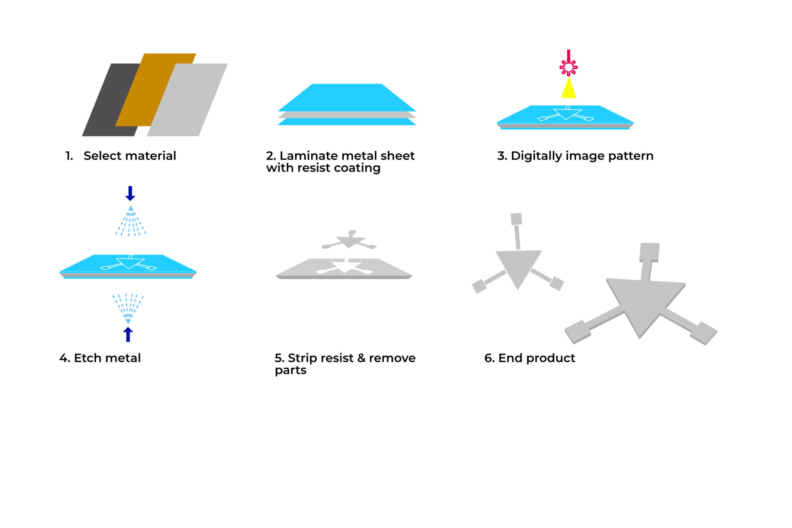
Known by many names, including photochemical machining, photo chemical etching, acid etching, chemical etching, photo etching, and photochemical milling, the photochemical etching process is a multi-step process that uses a light-sensitive polymer called photoresist to create a highly accurate mask that protects selected areas of the metal during etching. This process involves a thorough cleaning process and metal preparation to remove contaminants, ensuring optimal adhesion of the photoresist and precise chemical reactions during etching.
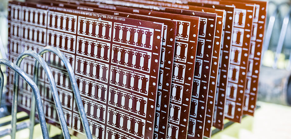
At Elcon Precision, our engineers digitally image the desired pattern onto a photoresist-coated metal substrate using advanced solid-state UV LED imaging technology. Mylar film and digital phototools are used to form the top and bottom halves of the phototool, ensuring precise alignment and masking of the sheet metal. The use of mylar film and digital phototools allows for quick, cost-effective tooling, with phototool costs typically in the hundreds of dollars compared to thousands for a stamping die, enabling rapid and inexpensive design revisions. The unexposed resist is removed, leaving only the precision mask pattern. After development, the remaining resist is stripped using an alkaline solution to reveal the bare metal for further processing. The sheet then passes through a controlled chemical etching system, where it enters an etching chamber, a multi-chambered machine equipped with conveyor systems and spray nozzles that uniformly apply the etchant, such as ferric chloride, from both sides of the metal sheet. The etchant’s oxidation-reduction potential is carefully monitored to control the chemical reactions and achieve precise dimensional tolerances, with the unprotected metal essentially corroding in the exposed areas to produce precise features with exceptional repeatability.
Because photochemical etching is a non-contact manufacturing process, the material type, including sheet metal and sheet metal components, retains its original metallurgical properties, grain structure, and physical characteristics, while eliminating burrs, stresses, and distortion commonly associated with traditional manufacturing methods like stamping, laser cutting, and mechanical machining.
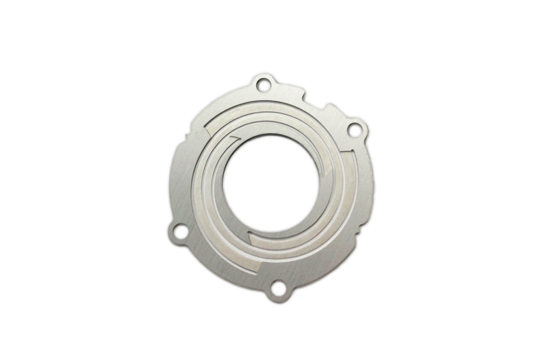
Our tightly controlled process variables allow Elcon to achieve dimensional tolerances as tight as ±0.0005 in., and photochemical etching can achieve tolerances as low as 0.001 inches (10 micrometers), making it ideal for producing complex, custom metal parts with tight tolerances, highly intricate geometries, fine pitch features, and delicate metal components across prototype through high-volume production.
With photochemical etching, increased part complexity does not increase tooling cost, making the process ideal for rapid prototyping, design iterations, and scalable production manufacturing. This process offers economical alternatives to traditional manufacturing methods, and the same process can be used for selective plating or other detailed applications, further enhancing its versatility in producing complex parts.
The Photochemical Etching Process
Elcon’s tailored photochemical etching process is engineered for repeatability, consistency, and precision from prototype through production volumes. Photochemical etching is a multi-step process with rigorous quality control and structured quality systems in place at every stage to ensure high precision and adherence to specifications. Each step, from cleaning and metal preparation to final inspection, is governed by strict quality systems to maintain dimensional accuracy and product quality.
Photoresist Coating
The cleaning process removes oils, rust, and contaminants as part of thorough metal preparation, ensuring the metal sheet is free from impurities. Achieving a smooth surface is essential for uniform photoresist adhesion and consistent etching results. Metal sheets are thoroughly cleaned and uniformly coated with a light-sensitive photoresist. This critical step ensures the metal surface is properly prepared for precise pattern transfer during imaging.
Imaging and Development
A digital phototool, consisting of top and bottom halves, is carefully aligned to both sides of the metal sheet to ensure precise masking during the photochemical etching process. Mylar film and digital phototools are commonly used for rapid and cost-effective pattern transfer, with mylar film offering quick revisions and affordability. UV light exposure transfers the pattern to the photoresist with exceptional accuracy. After exposure, the unexposed resist is developed away, revealing the bare metal (unprotected metal) in the areas to be etched, which defines the precise etch pattern.
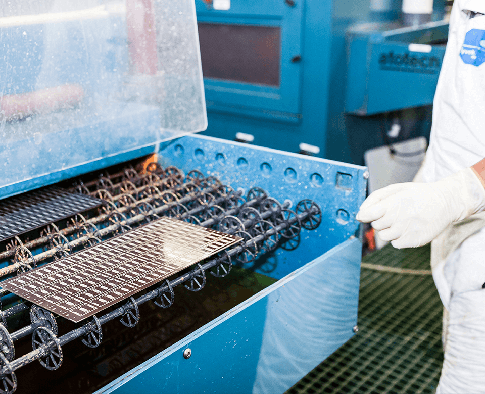
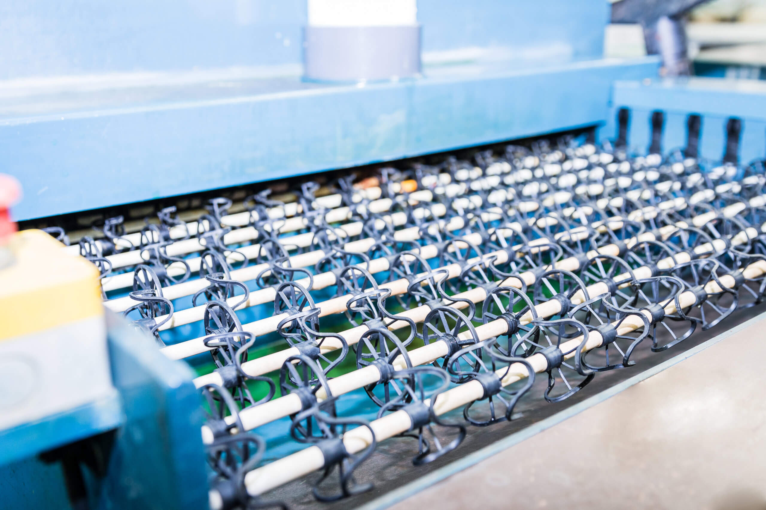
Controlled Chemical Etching
The patterned metal sheet passes through a precision-controlled chemical etching line where ferric chloride is used as the etchant. The etching chamber is a multi-chambered machine equipped with spray nozzles that deliver the etchant evenly onto the metal surface. During this step, the unprotected metal is essentially corroding in a controlled manner through carefully managed chemical reactions to form the desired features. The oxidation-reduction potential of the etchant is continuously monitored to control these reactions and ensure precise, high-quality etching. Process variables, including etchant concentration, temperature, spray pressure, and conveyor speed, are carefully controlled to ensure repeatable results.
This photochemical etching process produces burr-free, stress-free parts with smooth edges and highly accurate features. Elcon can manufacture parts with typical feature tolerances of ±10% of material thickness and process thin-gauge metals and foils ranging from 0.0005 in. to 0.100 in., depending on geometry.
Half etching and step etching can also be incorporated to create recessed features, bend lines, identification markings, and multi-level geometries.
Stripping, Inspection, and Finishing
Following etching, the remaining resist is stripped from the metal surface using an alkaline solution. Components are then inspected for dimensional accuracy, feature integrity, and compliance with customer specifications. Rigorous quality control and structured quality systems are implemented throughout this stage to ensure precise conformance to specifications and high product quality. Additional finishing services, including selective plating, passivation, forming, and brazing, may also be applied.
Throughout the photochemical machining process, Elcon emphasizes low-cost tooling, rapid turnaround, precision repeatability, and design flexibility. Multiple parts can be processed from a single sheet to maximize material utilization and manufacturing efficiency.
Industries & Applications
At Elcon Precision, we support mission-critical applications requiring advanced photochemical etching and precision metal fabrication across demanding industries, including:
- Defense and RF/vacuum electronics
- Aerospace and space systems
- Semiconductor manufacturing
- Photonics and optics
- Medical devices
- Nuclear and advanced energy
- Hydrogen and fuel cell technologies
Engineers across these industries rely on Elcon’s ability to translate highly complex designs into manufacturable, high-reliability precision metal components.
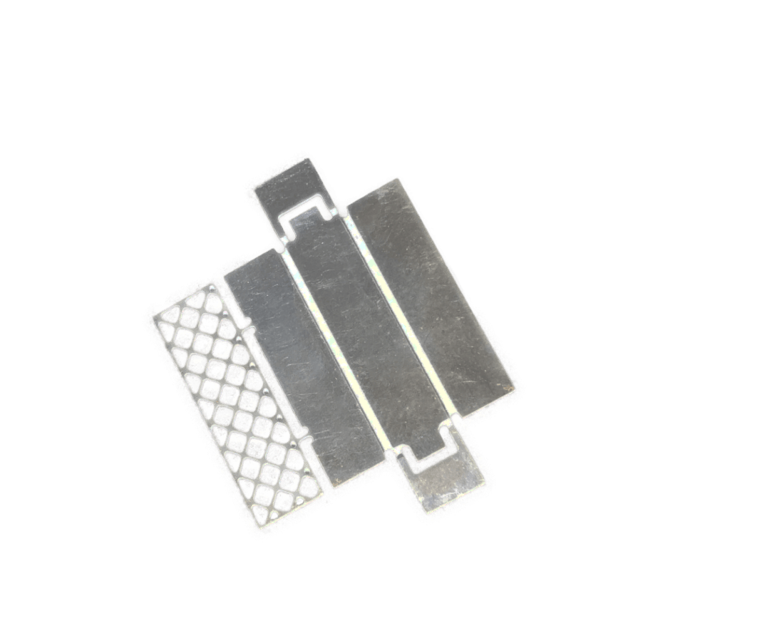
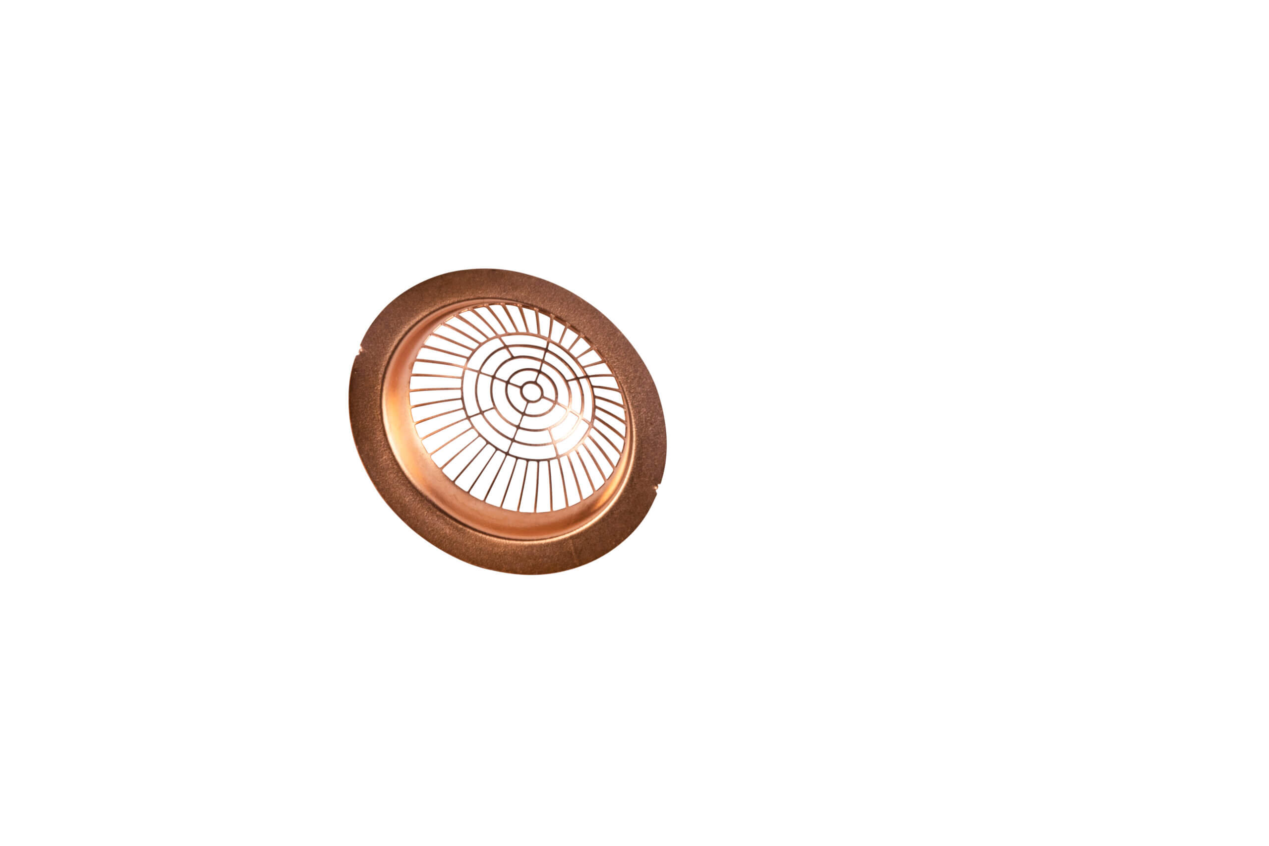
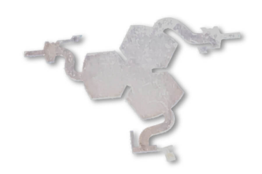
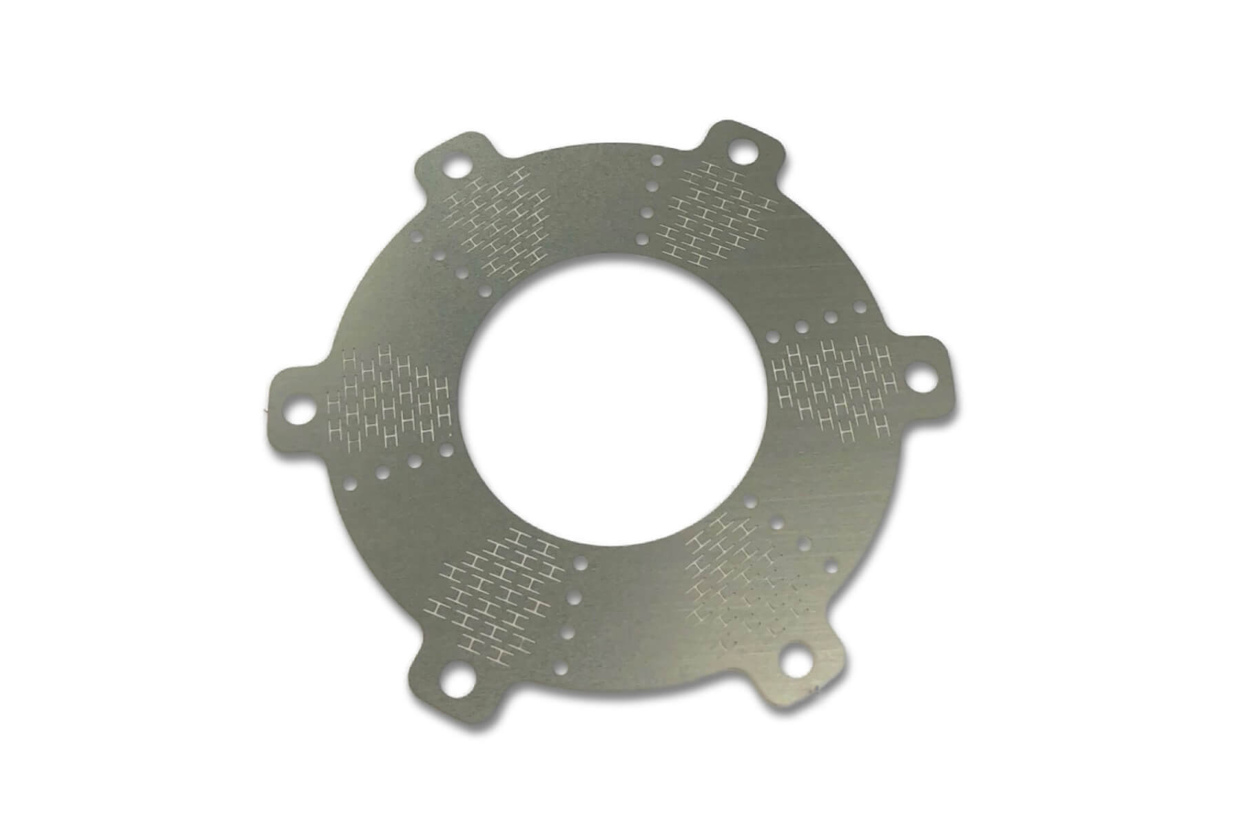
Photochemical etching is especially well-suited for applications requiring intricate geometries, thin metal sections, fine pitch patterns, tight tolerances, and burr-free edges.
Benefits
- Competitive cost
- Fast turnaround
- Burr-free, stress-free parts
- Low-cost tooling
- No heat-affected zones
- Metallurgical properties preserved
- Design flexibility
- Wide range of materials
- Dimensional repeatability
- Precise and complex geometries
- Ideal for prototyping and production
- Excellent for thin metals and fine features
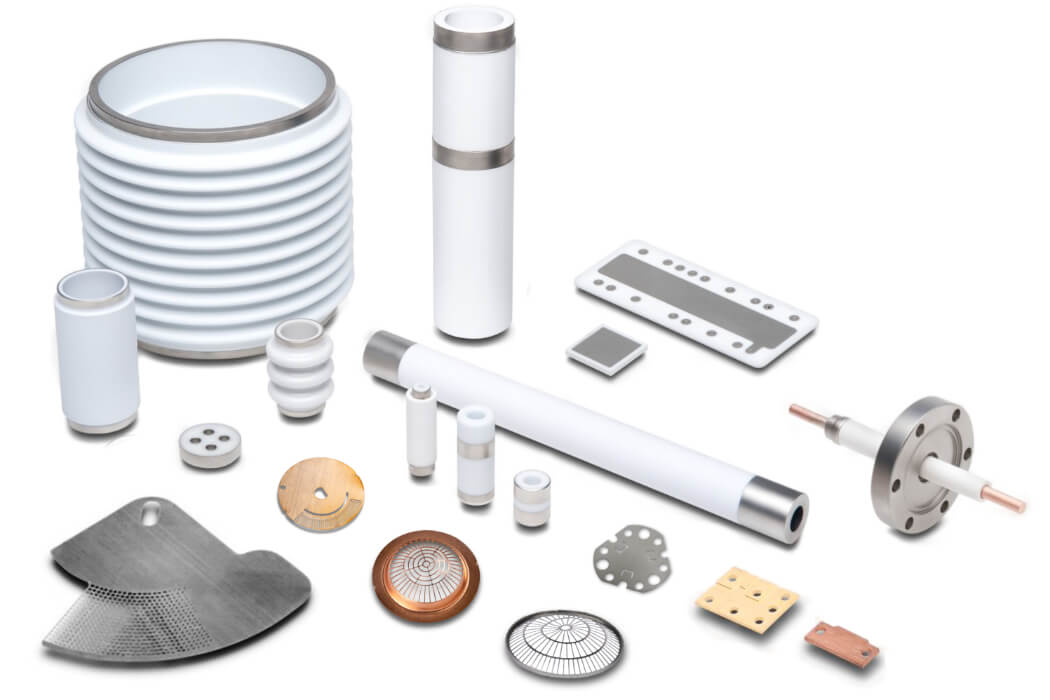
Capabilities
- Material thickness: 0.0005 in. to 0.100 in., depending on feature geometry
- Precision photochemical etching
- Photo chemical etching for thin metals and specialty alloys
- Step etching
- Half etching
- 3D photoetching
- Knife and needle edges
- Fine pitch and intricate geometries
- Selective plating
- Typical minimum hole diameter: 1.2x material thickness
- Typical minimum feature spacing: 1.2x material thickness
- Tight tolerances and dimensional repeatability
- Digital direct imaging for rapid design revisions
- See our Design Guidelines for more details
Applications:
- Fiber optics
- Heat exchangers
- RF shields, lids & carriers
- Optical encoders
- Lead frames
- Aerospace components
- Traveling wave tube (TWT) shadow and control hemispherical grids
- Vacuum electronics
- Microwave transmitting tubes
- Medical components
- Radiation shields
- Mesh for current collectors
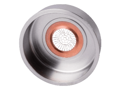
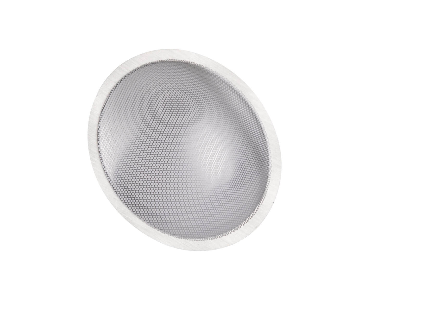
- Filters and screens
- Foil bearings
- Bipolar plates
- Semiconductor heater elements
- Precision apertures and masks
- EMI/RFI shielding
- Fuel cell components
Benefits
- Competitive cost
- Fast turnaround
- Burr-free, stress-free parts
- Low cost tooling
- Metallurgical properties preserved
- Design flexibility
- Wide range of materials
- Dimensional repeatability
- Precise and complex geometries
Capabilities
- Material thickness: 0.0005 in. to 0.100 in., depending on the features. Contact us with any questions!
- Step etching
- Half etching
- 3D photoetching
- Knife and needle edges
- Selective plating
- Typical minimum hole diameter: 1.2x material thickness
- Typical minimum feature spacing: 1.2x material thickness
- See our Design Guidelines for more detail.
Specifications
View applications for photochemical machining, the equipment we use, alternative naming conventions, and more below.


Ready to Explore What’s Possible?
Looking for a photochemical machining partner who understands your full system?
The team at Elcon Precision brings deep process knowledge, material expertise, and assembly integration under one roof, making us the best-value choice for complex, performance-driven applications.
We don’t just supply parts; we produce solutions that last the lifetime of your design.